Photo of Jawaharlal Pati

People · Current member

Jawaharlal Pati

PhD Scholar, Centre for Nanotechnology

Single metal-oxide nanowire devices and sensors

Jawaharlal fabricates electrical devices on single metal-oxide nanowires and modifies their surfaces for sensing applications. He is co-supervised by Prof. D. Pamu.

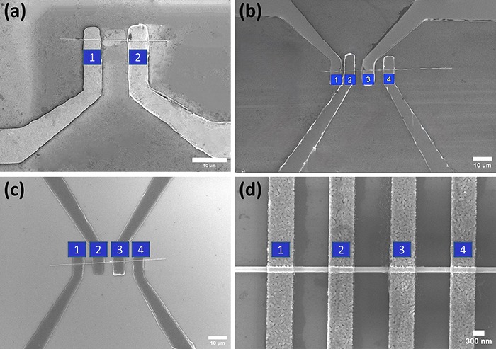
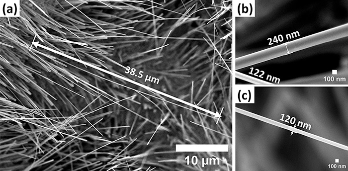
CuO nanowires (80–300 nm in diameter, 10–40 µm in length) are grown by thermal oxidation of copper foil. Individual wires are isolated, and 2-terminal, 4-terminal and transfer-length-method (TLM) structures are fabricated on them by laser and electron-beam lithography.

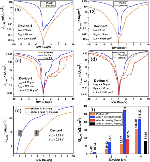
A short (7-minute) RF nitrogen plasma treatment increased the four-probe conductivity of single wires from 8–11 S/m to 40–105 S/m and reduced the turn-on voltage of 2-terminal devices from 1.75 V to 0.55 V. The increase scales with the surface-to-volume ratio, which indicates that nitrogen dopes only the surface region. Longer exposure roughens the surface and partially reduces CuO to Cu₂O, so that the conductance decreases again. TEM, single-wire Raman spectroscopy and EDX support this interpretation.
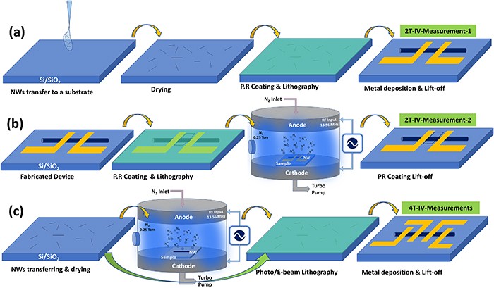
Single-nanowire device fabrication and N₂ plasma treatment
Single-nanowire device fabrication and N₂ plasma treatment. From J. Pati et al., J. Appl. Phys. 138, 024302 (2025), CC BY-NC-ND 4.0.
CuO nanowires grown by thermal oxidation of copper foil, and single wires of 120–240 nm diameter (FESEM)
CuO nanowires grown by thermal oxidation of copper foil, and single wires of 120–240 nm diameter (FESEM). From J. Pati et al., J. Appl. Phys. 138, 024302 (2025), CC BY-NC-ND 4.0.
2-terminal, 4-terminal and TLM devices fabricated on single CuO nanowires (FESEM)
2-terminal, 4-terminal and TLM devices fabricated on single CuO nanowires (FESEM). From J. Pati et al., J. Appl. Phys. 138, 024302 (2025), CC BY-NC-ND 4.0.
Current of single-nanowire devices before and after N₂ plasma treatment, showing a higher current and a lower turn-on voltage after 7 minutes
Current of single-nanowire devices before and after N₂ plasma treatment, showing a higher current and a lower turn-on voltage after 7 minutes. From J. Pati et al., J. Appl. Phys. 138, 024302 (2025), CC BY-NC-ND 4.0.

Education

  • PhD (ongoing), Centre for Nanotechnology, IIT Guwahati, co-supervised by Prof. D. Pamu, Dept. of Physics
  • M.Tech, Nanotechnology, IIT Patna

Publications

  1. Nitrogen plasma-induced conductivity enhancement of a single CuO nanowire J. Pati, P. Dobbidi, A. T. Mallajosyula Journal of Applied Physics 138, 024302 (2025) Open access · doi:10.1063/5.0261371