
Nanoelectronics and Semiconductor Devices Group · IIT Guwahati
Devices that harvest energy, emit light and remember
The group fabricates and models semiconductor devices based on halide perovskites, organic semiconductors and nanowires. The work extends from thin-film growth and device fabrication to defect spectroscopy, device simulation and circuit design.
Current devices include flexible perovskite memristors and crossbar arrays for neuromorphic computing, lead-free and tandem perovskite solar cells, green perovskite light-emitting diodes, and sensors based on single nanowires. More recent work addresses organic light-emitting diodes, a memristor-based artificial olfactory system, and energy-harvesting devices and circuits with supercapacitor storage. The group has also begun work on semiconductor packaging.
The aim is devices for real applications: memories and artificial synapses for low-power neuromorphic computing and wearable electronics, solar cells for outdoor, indoor and bifacial use, efficient light sources for displays, and sensors for health and environmental monitoring. The experimental work is supported by industry-standard TCAD and by CEISIM, a drift–diffusion simulator developed in the group for coupled electronic and ionic transport, which form the basis for analytical and compact models.
News
All news →- Talk by Prof. Subramanian Iyer (UCLA) on advanced packaging
- Abinash Baruah defends his PhD thesis
- Abdul Basit Andrabi presents his synopsis seminar
- IIT Guwahati and Tata Electronics sign MoU on semiconductor packaging
- Atanu Purkayastha awarded the ANRF National Post-Doctoral Fellowship
- Atanu Purkayastha defends his PhD thesis
- Rice University features Atanu Purkayastha
- Talk at IEEE PVSC 2024, Seattle
Research
All research →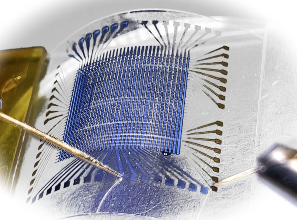 Memories
Memristors and neuromorphic hardware
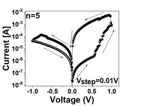
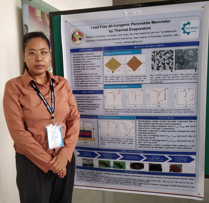
Halide perovskite resistive-switching memories on rigid and flexible substrates, integrated into crossbar arrays and artificial synapses for neuromorphic computing.
 Energy harvesting
Lead-free and tandem perovskite solar cells
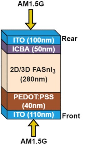
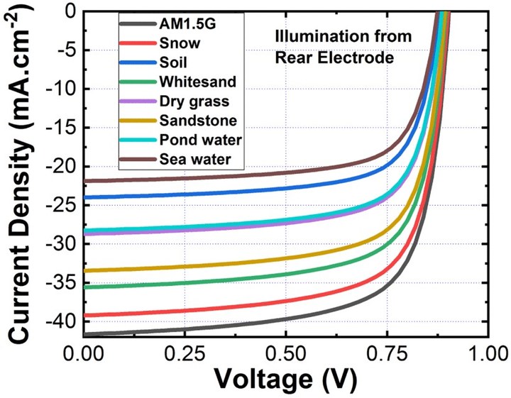
Tin-based perovskite solar cells, fabricated in the laboratory and extended through optical and electrical simulation to tandem, triple-junction and bifacial designs, with life-cycle assessment.
 Light emission
Perovskite and organic light-emitting diodes
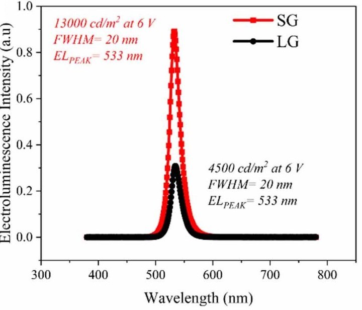
High-luminance, colour-pure green perovskite and organic LEDs, and the ion migration and trap physics that limit their luminous efficiency and operational lifetime.
 Nanodevices
Nanowire devices and sensors
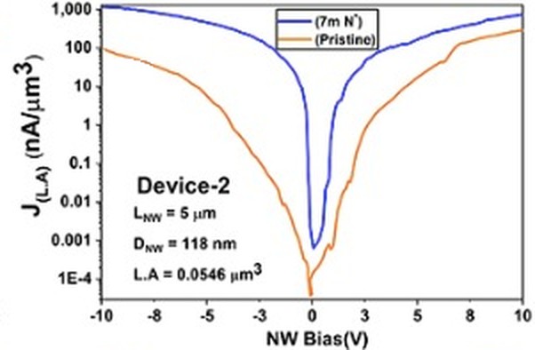
Electrical devices on single metal-oxide nanowires with plasma-modified surfaces for sensing applications, and nanodevices that combine energy generation and storage.
 Device physics
Defect spectroscopy and device modelling
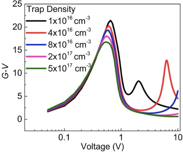
Physics-based methods to characterise traps and mobile ions in perovskite devices from electrical measurements, an in-house device simulator, and compact models.
 Packaging
Semiconductor packaging
Advanced packaging for flexible electronics and MEMS, and the integration of micro- and nano-fabrication steps into complete packaged devices.
Recent papers
All publications →- Integrating dimensional engineering and optical management for high-performance lead-free all-perovskite tandem solar cells Solar Energy Materials and Solar Cells 297, 114100 (2026) · doi:10.1016/j.solmat.2025.114100
- Multiscale dielectric relaxation and trap-assisted conduction in halide perovskite light-emitting diodes Journal of Physics D: Applied Physics 59, 015112 (2026) · doi:10.1088/1361-6463/ae27de
- Giant polarization facilitating ion migration in perovskite light emitting diodes: implications for performance degradation Journal of Physics D: Applied Physics 58, 205105 (2025) · doi:10.1088/1361-6463/adcd82
- Nitrogen plasma-induced conductivity enhancement of a single CuO nanowire Journal of Applied Physics 138, 024302 (2025) Open access · doi:10.1063/5.0261371
Our research is funded by






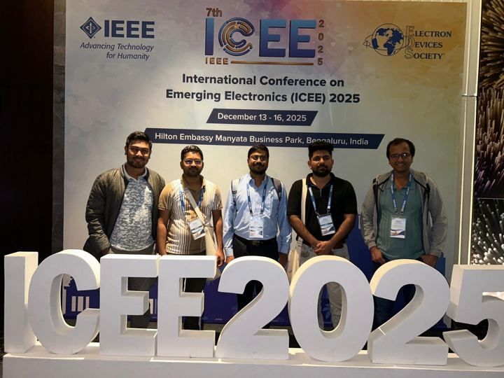
Life in the group
Gallery →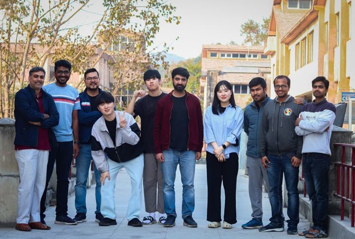

Join us
The group welcomes applications from prospective PhD, M.Tech and B.Tech students, postdoctoral researchers and interns with an interest in device fabrication and device physics. Please write to Dr. Arun Tej Mallajosyula with a CV and a short statement of research interests.