

Owing to their large surface-to-volume ratio, the current in nanowires is highly sensitive to changes at the surface. Single nanowires are therefore promising as sensing elements, provided that reliable contacts can be formed and the surface can be controlled.
Key results
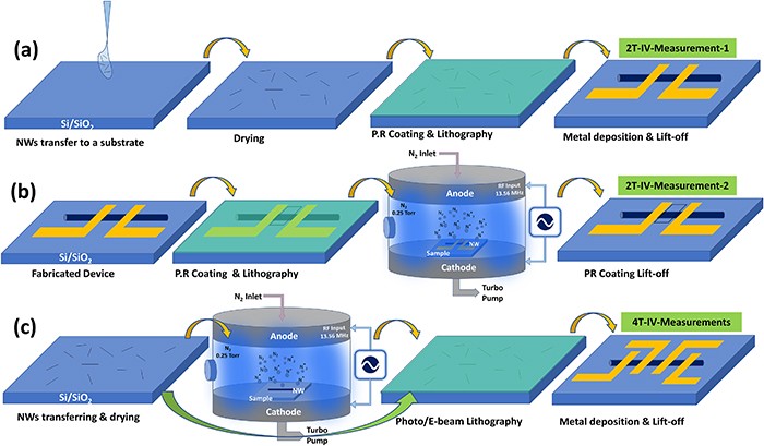
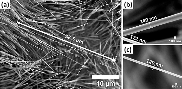
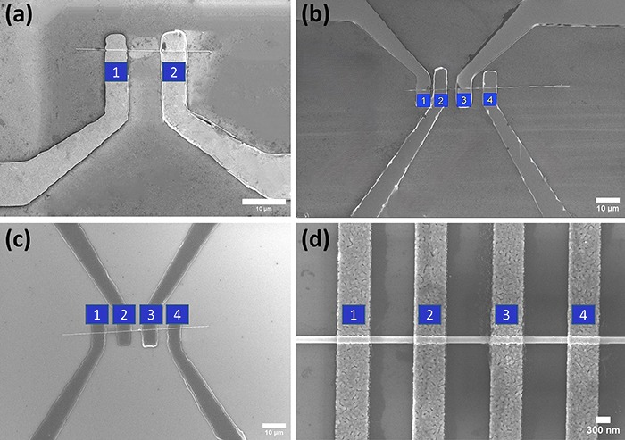
- Single-nanowire devices. CuO nanowires grown by thermal oxidation of copper are isolated individually, and 2-terminal, 4-terminal and TLM structures are patterned on them by laser and electron-beam lithography.
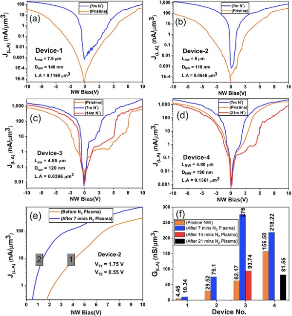
- Plasma surface doping. A 7-minute RF nitrogen plasma treatment increased the conductivity of single wires from 8–11 S/m to 40–105 S/m. The larger increase in thinner wires indicates that the doping is confined to the surface. Longer exposure damages the surface and reduces the conductance.
Work on nanodevices that combine energy generation and storage is in progress.
Methods and tools
Thermal oxidation growth · laser and e-beam lithography · RIE nitrogen plasma · single-wire Raman · TEM and EDX · 2- and 4-probe I–V · transfer length method