

Halide perovskites emit light with a narrow linewidth, and the emission wavelength can be tuned through the halide composition, which makes them attractive for display applications. Their principal limitation is operational lifetime. The mobile ions that facilitate low-temperature processing also migrate under bias and degrade the device. We fabricate green MAPbBr₃ LEDs and investigate the role of mobile ions and traps using electrical spectroscopy.
Approach
Perovskite LEDs already exhibit high luminance and colour purity, owing to a high photoluminescence quantum yield, a composition-tunable band gap and low-cost solution processing. Their development is, however, limited by operational stability and device-to-device reproducibility. The underlying causes, including ion migration, trap-assisted recombination and interfacial instability, are not yet fully understood.
PeLEDs are fabricated in the clean room and characterised as electronic devices using:
- Temperature-dependent impedance spectroscopy
- Current–voltage measurements under bias stress
- Deep-level transient spectroscopy (DLTS)
These measurements reveal ion migration, the evolution of trap states and the response of the bulk and interfaces during operation. We also study the self-healing of the perovskite layer when the device is rested, which is directly relevant to lifetime. The aim is to relate materials science to device engineering and to establish design guidelines for more stable and efficient PeLEDs.
Key results
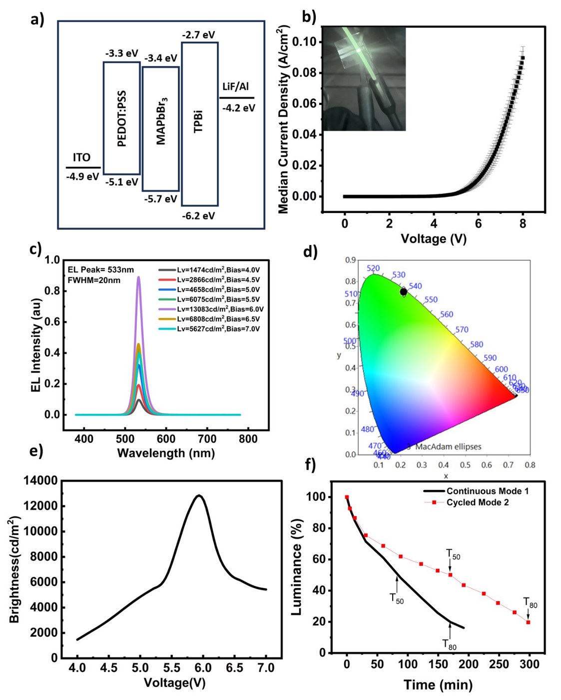
- Green emission with high colour purity. A luminance of up to 13,000 cd/m² at 6 V, with an emission peak at 533 nm and a FWHM of 20 nm.
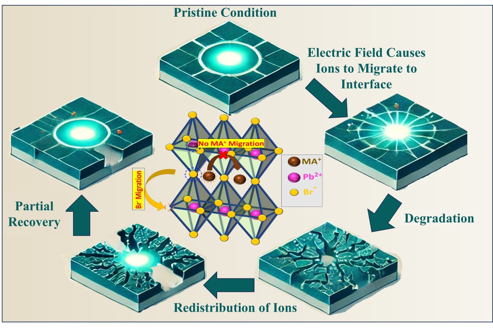
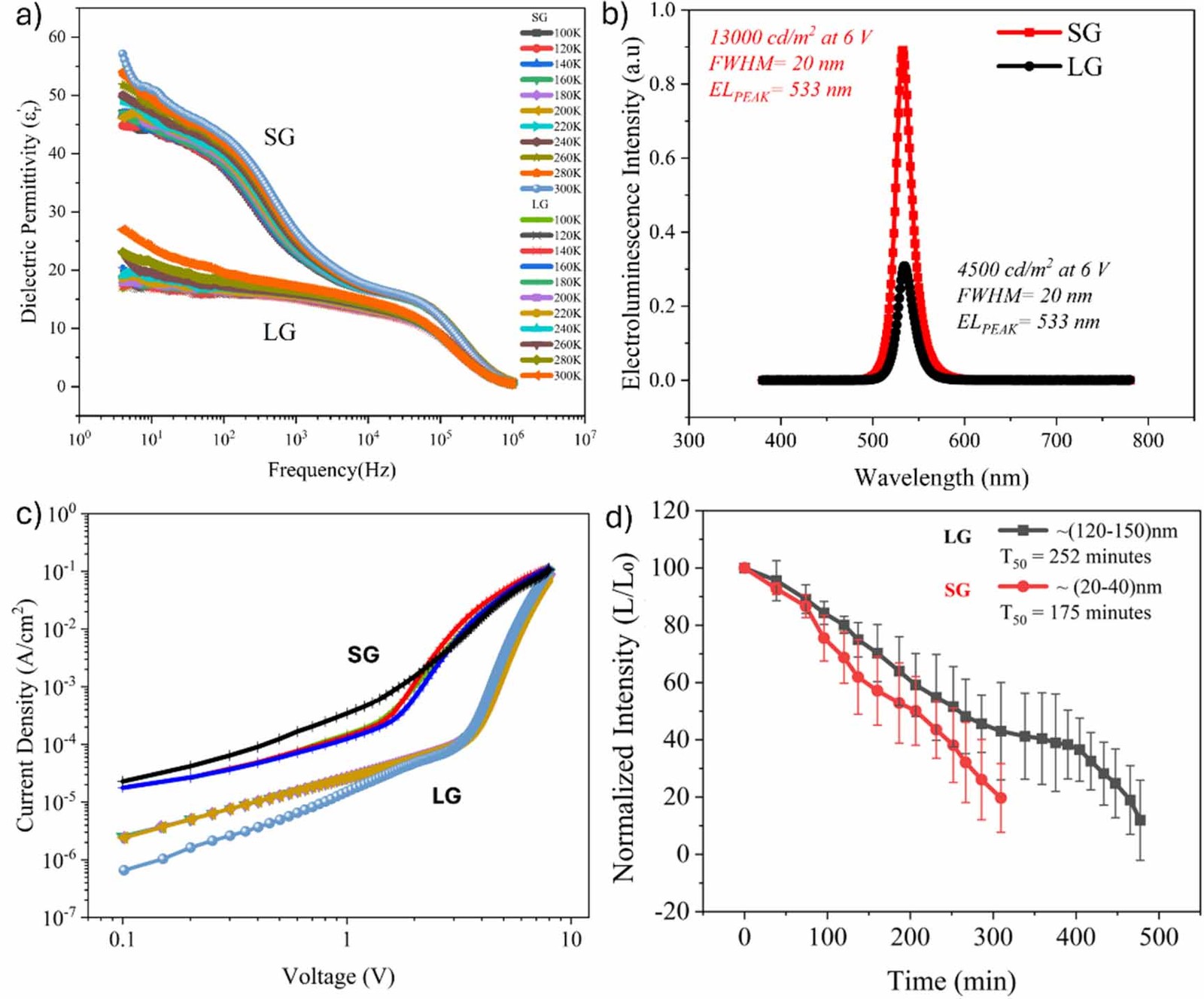
- Ion migration as the degradation mechanism. Under bias, Br⁻ ions accumulate at the anode, as confirmed by cross-sectional EDX. This accumulation gives rise to a giant apparent permittivity at low frequency. During rest, the ions partially redistribute, and cycled operation approximately doubles the T₅₀ lifetime. The ion diffusion coefficient, mobility and density were extracted from impedance data.
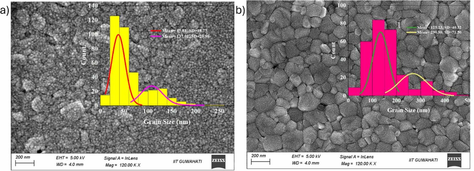
- Effect of grain size. Small grains (~62 nm) yield higher luminance and a lower turn-on voltage but a shorter lifetime (T₅₀ 175 min), whereas large grains (~150 nm) yield a longer lifetime (T₅₀ 252 min). Mobile charge stored at grain boundaries is found to facilitate carrier injection and to accelerate degradation.
- Transport and traps. Conduction is consistent with correlated barrier hopping. DLTS reveals a shallow trap at 0.30 eV, attributed to bromide-vacancy-related ionic defects.
Work on organic LEDs is in progress.
Methods and tools
Solution processing · electroluminescence and luminance (Konica Minolta CS-2000) · temperature-dependent impedance (77–380 K) · electric modulus and universal dielectric response analysis · DLTS · FESEM and cross-section EDX