
Research · Device physics

Defect spectroscopy and device modelling

Physics-based methods to characterise traps and mobile ions in perovskite devices from electrical measurements, an in-house device simulator, and compact models of transistors and memories.

The behaviour of perovskite memories, solar cells and LEDs is strongly influenced by defects, namely deep and shallow traps and mobile ions. Their characterisation is difficult because their signatures overlap in conventional electrical measurements. We develop methods to distinguish these contributions, validate the methods against device simulation, and establish the conditions under which each interpretation is reliable.

Approach

For each device that we fabricate or simulate, the aim is to understand the underlying physics and to express it in analytical or semi-empirical models. We study generation and recombination, and both electronic and ionic charge transport, using nano-scale imaging, deep-level transient spectroscopy, impedance spectroscopy, and low-temperature I–V and C–V measurements. Device structures are simulated with Synopsys Sentaurus and Silvaco 2D/3D TCAD, Lumerical and MATLAB, both to support the experiments and to develop new models.

Key results

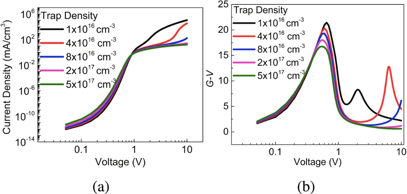
  • Trap characterisation from dark J–V characteristics. Trapped charge near the injecting contact causes band bending, which shifts the diffusion-to-drift transition voltage (the peak of d log J / d log V) to lower values. In simulation, this shift follows the trap density and depth in the presence of mobile ions, and distinguishes films more reliably than VOC.
  • CEISIM, an in-house simulator. CEISIM (Coupled Electronic–Ionic Transport Semiconductor Device Simulator) is a one-dimensional drift–diffusion simulator that treats trap occupancy and mobile ions as dynamical variables, with DC, small-signal and transient solvers in a single framework. It provides access to the internal state of the device during impedance and transient measurements.
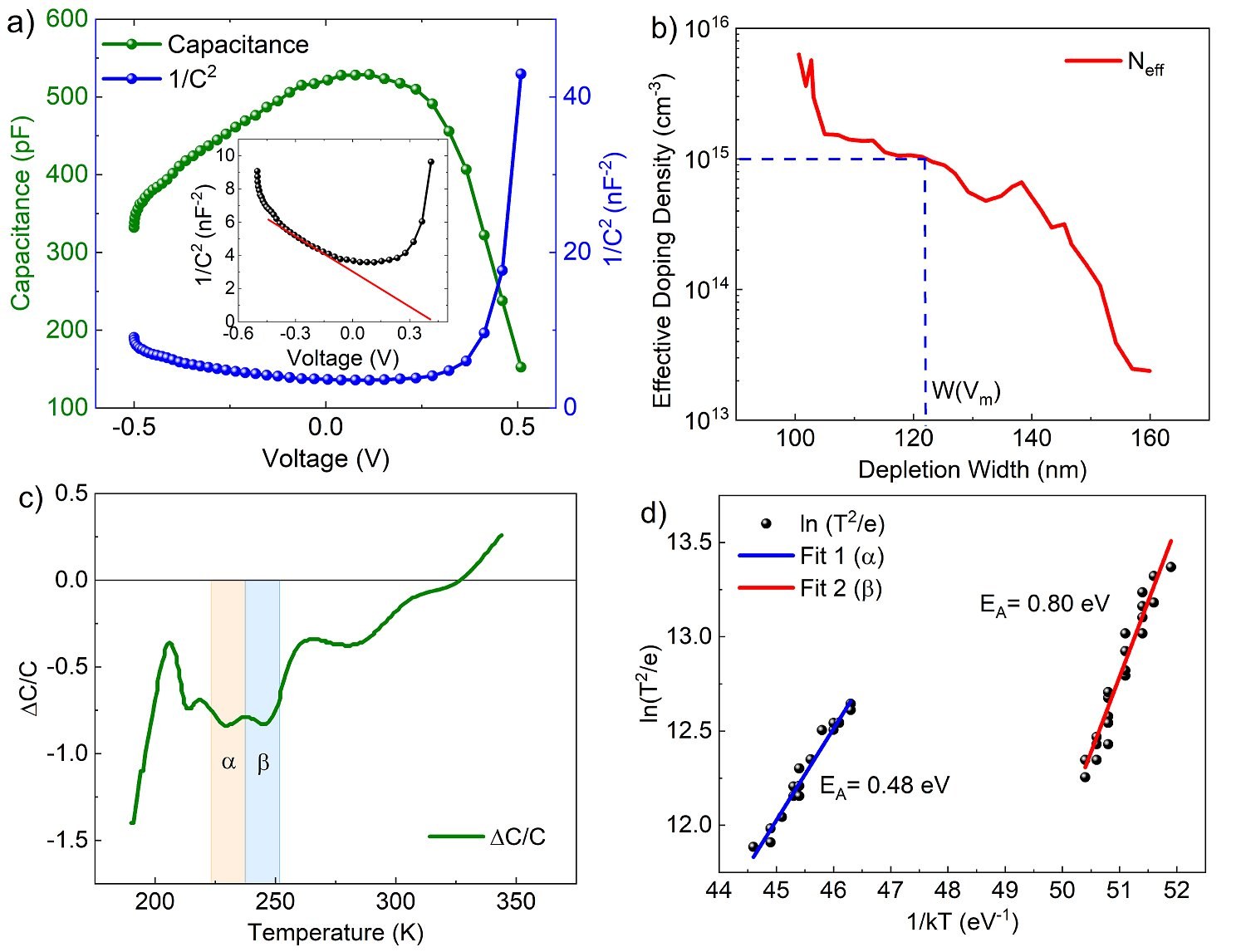
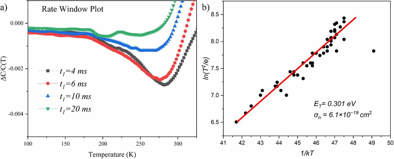
  • DLTS of ionic defects in perovskite memristors (methylammonium vacancies, 0.48 eV) and LEDs (a bromide-vacancy-related trap, 0.30 eV).
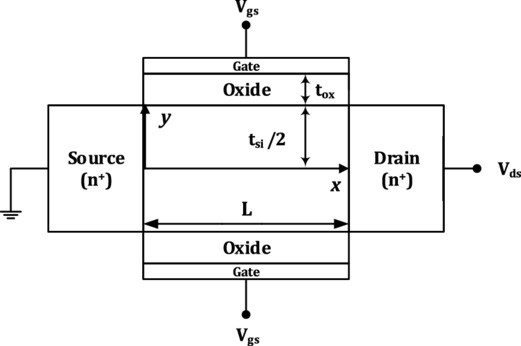
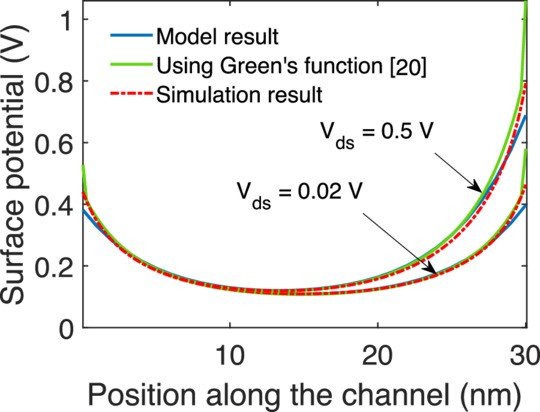
  • Compact models. An analytical model of the double-gate MOSFET for the channel potential, subthreshold current and drain current, and a simulation study of a pore-confined phase-change memory that uses current crowding to reduce programming energy.
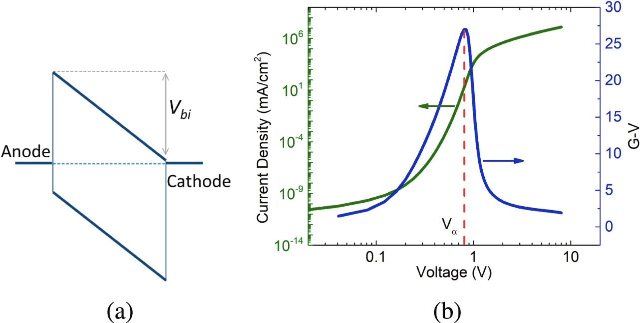
The transition voltage, at which the slope of log J against log V peaks and the current changes from diffusion-dominated to drift-dominated
The transition voltage, at which the slope of log J against log V peaks and the current changes from diffusion-dominated to drift-dominated. From A. B. Andrabi and A. T. Mallajosyula, Sol. Energy 264, 112020 (2023).
TCAD simulation showing the shift and weakening of the transition peak with increasing trap density
TCAD simulation showing the shift and weakening of the transition peak with increasing trap density. From A. B. Andrabi and A. T. Mallajosyula, Sol. Energy 264, 112020 (2023).
C–V characteristics, doping profile and DLTS of a flexible perovskite memristor, showing ionic defect levels
C–V characteristics, doping profile and DLTS of a flexible perovskite memristor, showing ionic defect levels. From H. J. Gogoi, A. B. Andrabi et al., IEEE IFETC (2022).
DLTS rate-window scan and Arrhenius plot of a deep trap in a perovskite LED
DLTS rate-window scan and Arrhenius plot of a deep trap in a perovskite LED. From A. Baruah and A. T. Mallajosyula, J. Phys. D 59, 015112 (2026).
Double-gate MOSFET structure used for the compact model
Double-gate MOSFET structure used for the compact model. From R. U. Ahmed and A. T. Mallajosyula, Phys. Scr. 100, 085414 (2025).
Surface potential along the channel from the model and from TCAD simulation
Surface potential along the channel from the model and from TCAD simulation. From R. U. Ahmed and A. T. Mallajosyula, Phys. Scr. 100, 085414 (2025).

Methods and tools

Sentaurus and Silvaco TCAD · CEISIM (our in-house 1D drift–diffusion simulator) · DLTS · impedance and capacitance spectroscopy · low-temperature I–V and C–V · MATLAB

Papers in this area

  1. Multiscale dielectric relaxation and trap-assisted conduction in halide perovskite light-emitting diodes A. Baruah, A. T. Mallajosyula Journal of Physics D: Applied Physics 59, 015112 (2026) · doi:10.1088/1361-6463/ae27de
  2. Efficient and accurate modeling of double-gate MOSFETs: a computationally feasible approach for potential, subthreshold, and drain current characteristics R. U. Ahmed, A. T. Mallajosyula Physica Scripta 100, 085414 (2025) · doi:10.1088/1402-4896/adf5f6
  3. Unraveling trap distribution in perovskite films: a qualitative analysis via diffusion to drift transition voltage of current–voltage characteristics A. B. Andrabi, A. T. Mallajosyula Solar Energy 264, 112020 (2023) · doi:10.1016/j.solener.2023.112020
  4. Trap-mediated ionic dynamics in MAPbBr₃ PeLEDs revealed by modulus and deep-level transient spectroscopies A. Baruah, A. T. Mallajosyula 10th IEEE Electron Devices Technology & Manufacturing Conference (EDTM) (2026) · doi:10.1109/EDTM65772.2026.11496963
  5. Energy-efficient pore-confined phase change memory using current-crowding effect: a simulation study R. U. Ahmed, A. T. Mallajosyula, B. Saini, U. Ganguly VLSI Design and Test (VDAT), Springer CCIS 459–472 (2026) · doi:10.1007/978-3-032-26305-6_36
  6. Ionic defect analysis in flexible hybrid perovskite memristor using deep level transient spectroscopy H. J. Gogoi, A. B. Andrabi, M. R. Sekhar, A. T. Mallajosyula IEEE International Flexible Electronics Technology Conference (IFETC) (2022) · doi:10.1109/IFETC53656.2022.9948530
  7. Analysis of ionic defects in hybrid perovskite memristors using deep level transient spectroscopy H. J. Gogoi*, A. B. Andrabi*, A. T. Mallajosyula 1st International Conference on Low-Energy Digital Devices and Computing (ICLED), Singapore (2023)