

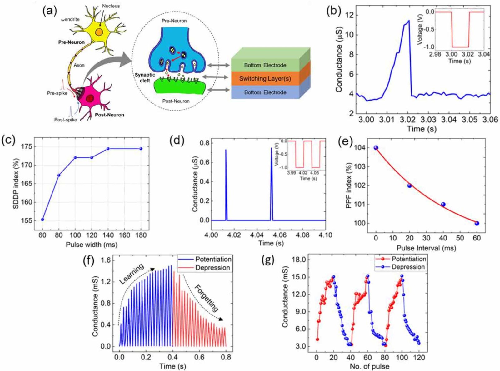
A memristor is a two-terminal device whose resistance can be switched between a high-resistance and a low-resistance state and is retained without power. In halide perovskites, switching is attributed to the formation and rupture of a conducting filament by mobile ions and vacancies. These memories are low-cost, operate at low voltages and can be fabricated on flexible substrates. As their conductance can be modulated in small increments, they can also emulate biological synapses.
Background
A memristor is non-volatile, exhibits a pinched hysteresis loop in its I–V characteristics and can support multiple resistance levels in addition to binary states. These properties enable multi-bit storage, in-memory computing and devices that emulate synaptic weights. Since the conductance can be incrementally increased or decreased, memristors can exhibit spike-timing-dependent plasticity and Hebbian learning. Switching energies as low as the femtojoule range have been reported, well below those of SRAM and DRAM, and the two-terminal structure is well suited to dense 3D crossbar integration.
Applications include non-volatile memory, neuromorphic and in-memory computing, physically unclonable functions (PUFs), analog signal processing and logic-in-memory. Broader directions in the field include 3D memristor arrays (3D RRAM, VRRAM), edge-AI hardware for wearable and IoT devices, radiation-tolerant memory for space applications, and stochastic neuromorphic systems. Our work focuses on flexible, high-endurance crossbar RRAMs based on emerging materials such as halide perovskites.
Key results
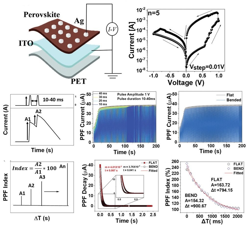
- Lead-free, flexible and air-stable memristors. Cs₃Bi₂I₉ memristors on PET show an ON/OFF ratio above 10⁵ and an endurance of 10⁴ cycles. They remain functional after more than 30 days at over 80% relative humidity without encapsulation, and under bending to a 5 mm radius. A flexible 4×4 crossbar array was fabricated with 81% device yield. The devices exhibit synaptic potentiation and depression at about 0.1 µJ per event.
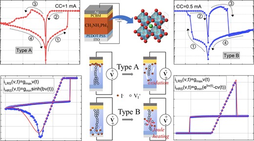
- Two switching modes in a single cell. In MAPbI₃ memristors, the compliance current selects between a field-driven (redox) mode and a Joule-heating mode of opposite polarity. In combination, the two modes provide complementary resistive switching in a single cell, which can suppress sneak currents in crossbar arrays.
- Measurement methodology. The scan rate, compliance current, pulse parameters and device area all influence the switching voltages and the ON/OFF ratio. These dependences were characterised systematically, and a standard measurement protocol was proposed.
- Defects involved in switching. DLTS on flexible MAPbI₃ memristors identifies methylammonium vacancies (activation energy of about 0.48 eV) that are expected to assist filament formation.
- From device to array. M.Tech projects have addressed the design of read/write peripheral circuits for passive ReRAM crossbars at the 180 nm and 65 nm nodes, as well as sneak-path currents and crosstalk.
Ongoing work includes larger crossbar arrays based on all-inorganic perovskites and a memristor-based artificial olfactory system.

Methods and tools
Spin coating and thermal / e-beam evaporation · conductive AFM · DC and pulsed I–V (Keysight B1500A, Keithley 4200) · DLTS · SPICE (Yakopcic) models · ReRAM peripheral circuits at 180 nm and 65 nm